∫ f(x)dxE = mc²∇ × E = -∂B/∂tπ ≈ 3.1416F = G(m₁m₂)/r²d/dx (eˣ) = eˣ


Admissions Open for HSC Batches
Empowering SSC, HSC & Engineering Aspirants
Loading page...4%
Empowering SSC, HSC & Engineering Aspirants
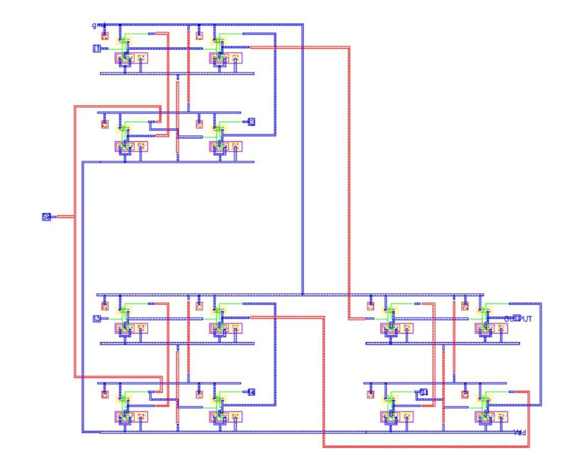
Designed a 4×1 MUX using three 2×1 multiplexer blocks with two select lines to route one of four inputs to a single output. Implemented the design in 240 nm CMOS technology, including NAND, 2×1 MUX, and final 4×1 MUX layouts. Verified the physical design through DRC, LVS, and RCX, then validated functionality using post-layout simulation with extracted parasitics. Used Cadence Virtuoso for schematic, layout, extraction, and waveform-based verification of the final circuit.
Detailed technical documentation, implementation strategies, and outcome analysis for this project are currently being compiled. This section will be updated with comprehensive insights into the methodologies, challenges overcome, and the ultimate impact of the developed solution.